Facilities - equipment listing
Training Request Form iLab Calendar Access Account Set-Up/Renewal
The majority of the IMSE user facilities are located in the basement of Rudolph Hall (Earth, Environmental, and Planetary Sciences), including a 12,000 net sq ft facility opened in Fall 2013 which includes a micro- and nanofabrication facility and a materials characterization facility. These facilities are available for use by researchers from all WashU schools and departments, as well as to users from other universities, government laboratories and industry.
For external rates please contact Beth Gartin.
Materials Characterization Facility
Atomic Force Microscope (AFM) | Bruker Dimension ICON AFM

Atomic Force Microscope (AFM) Bruker Dimension Icon
- Tunneling AFM (TUNA)
- Kelvin probe force microscopy (KPFM)
- Quantitative nanoscale mechanical (QNM) characterization
- Photoconductive AFM (pcAFM)
Book a Reservation/Equipment Availability - Request Training
IMSE Contact & Approved Trainers:
Dr. Huafang Li Hli40@wustl.edu
Dr. Tyrone Daulton TDaulton@wustl.edu
Training Materials:
N/A
Technical Information:
N/A
Environmental Scanning Electron Microscope (ESEM) | Thermofisher Quattro S ESEM
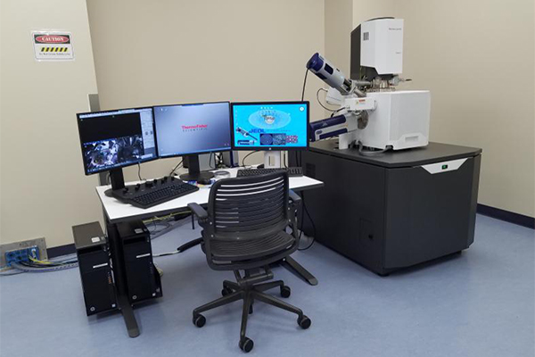
Thermofisher Quattro S ESEM
- Electron Source: High-stability Schottky field emission gun.
- Electron Resolution: 0.7 nm at 30 keV, 1.4 nm at 1 keV.
- Everhart-Thornley secondary electron (SE) Detector, segmented solid-state backscatter electron (BSE) detector, and Low Vacuum (LVD) detector.
- In-chamber Nav-Cam sample navigation camera.
- Variable pressure operation.
- Environmental pressure operation (ESEM).
- Oxford AzTec Energy Dispersive X-ray Spectrometer (EDXS).
- Oxford Symmetry Electron Backscattered Detector (EBSD).
- Bruker PI88 Nanoindentor.
Book a Reservation/Equipment Availability - Request Training
IMSE Contact & Approved Trainers:
Dr. Huafang Li Hli40@wustl.edu
Dr. Tyrone Daulton TDaulton@wustl.edu
Training Materials:
Technical Information:
N/A
Scanning Transmission Electron Microscope (STEM) | JEOL JEM-2100F Field-Emission STEM
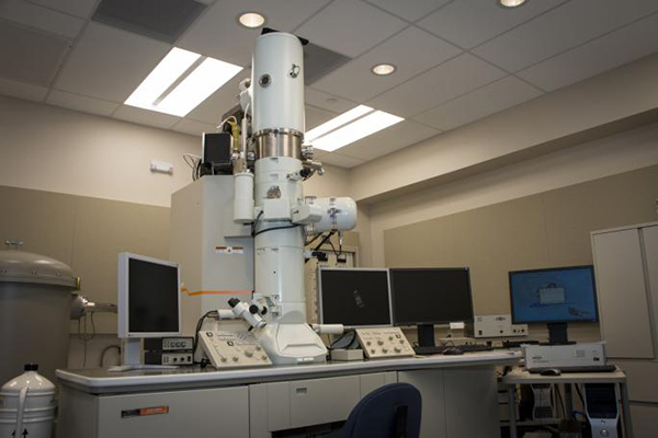
JEOL JEM-2100F Field-Emission STEM
Access JEM-2100F Field-Emission STEM Training Materials
Training Contact: Dr. Huafang Li hli40@wustl.edu
Maintenance Contact: Dr. Tyrone Daulton tdaulton@physics.wustl.edu
- High brightness Schottky field emitter
- Resolution: 0.23 nm point-to-point, 0.1 nm lattice; high-resolution pole piece
- Bright field (BF), dark field (DF), and high-angle annular dark-field (HAADF) detectors
- High resolution lattice imaging (HRTEM)
- Bruker SDD Energy Dispersive X-ray Spectroscopy (EDXS) system
- Gatan Tridiem electron energy imaging filter (GIF) system for Electron Energy Loss Spectroscopy (EELS)
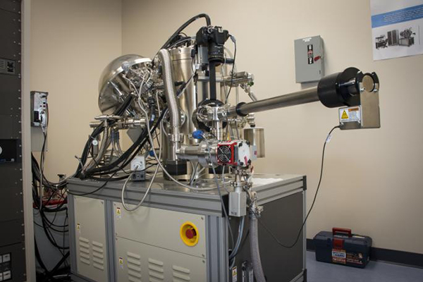
Focused Ion Beam FIB | Thermofisher Scios 2 DualBeam FIB
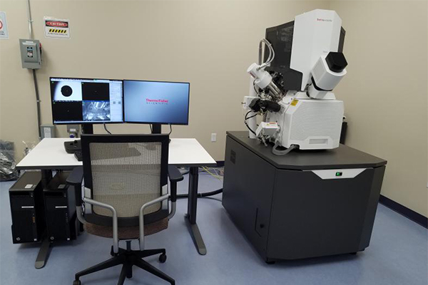
Thermofisher Scios 2 DualBeam FIB
- Electron Source: High-stability Schottky field emission gun
- Electron Resolution: 0.7 nm at 30 keV, 1.4 nm at 1 keV
- Ion Source: Sidewinder ion column
- Ion Resolution: 3.0 nm at 30 kV using selective edge method
- Everhart-Thornley secondary electron (SE) Detector and retractable, segmented solid-state backscatter electron (BSE) detector
- Platinum Gas injection
- Thermo Scientific EasyLift system for in situ sample manipulation
- FIB charge neutralizer
- In-chamber Nav-Cam sample navigation camera
- Variable pressure operation
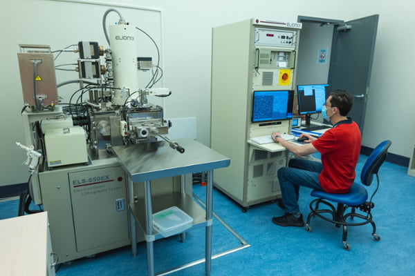
Elionix ELS-S50EX Electron Beam Lithography (EBL)
Book a Reservation/Equipment Availability - Request Training
IMSE Contact & Approved Trainers:
Dr. Tyrone Daulton TDaulton@wustl.edu
Training Materials:
N/A
Technical Information:
N/A
Transmission Electron Microscope (TEM) | JEOL JEM-2000 FX TEM
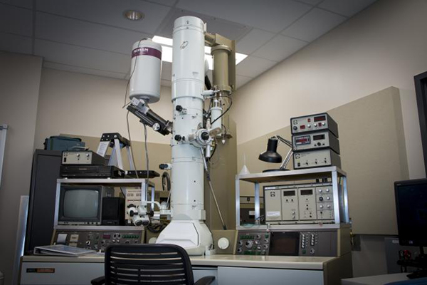
JEOL JEM-2000 FX TEM
Access 2100 TEM Training Materials
Primary points of contact:
New User Training: Dr. Huafang Li hli40@wustl.edu
Maintenance: Dr. Tyrone Daulton tdaulton@physics.wustl.edu
- LaB6 Emitter
- ThermoNoran Energy Dispersive X-ray Spectroscopy (EDXS) system
- Gatan Model 666 parallel electron energy loss spectrometer (PEELS) system
Thermo Mechanical Analyzer (TMA) | Mettler Toledo, Model TMA/SDTA 840

Mettler Toledo, Model TMA/SDTA 840
Contact: Dr. Huafang Li hli40@wustl.edu
314-935-8701
- Temperature-dependent mechanical property measurement (max. applied load 1 N) up to 1100 °C
- Measure the thermal expansion of solid samples with 5 nm resolution
- Detect phase transformations, including amorphous-crystalline, crystalline-crystalline and melting events
X-Ray/Ultraviolet Photoelectron Spectrometer (XPS) | Physical Electronics 5000 VersaProbe II Scanning ESCA Microprobe
Physical Electronics 5000 VersaProbe II Scanning ESCA Microprobe
Contact: Dr. Huafang Li hli40@wustl.edu
314-935-8701
- Al K-alpha x-ray source to help determine chemical states of surfaces a few nanometers deep
- He I and II ultraviolet sources to provide information on the valence band of materials
- Mapping and imaging capabilities in the XY direction; Ar sputtering allows depth analysis
- Glove box with a portable transfer chamber for preparing air or O2 sensitive samples
- Hot/cold stage (500 °C/-100 °C) available
X-ray Powder Diffraction (XRD) | Rigaku D-Max-B Powder Diffractometer

Rigaku D-Max-B Powder Diffractometer
Contact: Dr. Tyrone Daulton tdaulton@wustl.edu
314-935-4537
- Cu K-alpha x-ray source
- 1.5 kV power supply
- Special attachment for limited high temperature operation
Microfabrication and Nanofabrication
Acid Fume Hood
Acid Fume Hood
The Acid Fume hood located in the Class 100 Cleanroom allows wet etching of nanometer scale features in different substrate materials including Silicon wafers. A buddy system is required in most operations. Additional training is required before any independent use. The training is documented in the Bluebook. IMSE provides the necessary PPE for safe use of chemicals.
Book a Reservation/Equipment Availability - Request Training
IMSE Contact & Approved Trainer:
Dr. Huafang Li (hli40@wustl.edu)
Following chemicals are supplied by IMSE (and are included in your rate):
- Buffered Oxide Etchant
- Hydrofluoric Acid (48%)
- Aluminum Etchant Type D
- Chromium Etching 1020
- Gold Etchant
- Nitric Acid (70%)
- Sulfuric Acid (95%)
- Hydrochloric acid (37%)
- Hydrogen Peroxide
- Phosphoric Acid
- Acetic Acid
- Ferric Chloride
The following chemicals are in use by other PIs (will require additional permission from PIs before use):
- Indium Tin Oxide Etching TE-100
- Aluminum Etchant Type A
Training Documents:
NOTE: User must demonstrate skills to IMSE staff before independent use (Acid hood training form).
Personal Protective Equipment (Acid Use)
Acid Waste Handling
Training Videos
HydroFluoric (HF) Acid
Cr 1020 Etchant
Pirahna etch
RCA Clean
HF/HNO3 mixtures
Recipe:
Click here to see available recipes
Technical Info:
Safety Data Sheets of chemicals
Acid Fume Hood (outside of Cleanroom)
Book a Reservation/Equipment Availability - Request Training
The Acid hood has the capability to handle any number of acids and wet etchants. This is located in Lab L27 (outside cleanroom). Waste is handled in a controlled and safe manner. Additional DI water is available for high purity applications.
IMSE Contact & Approved Trainer:
Training Documents:
NOTE: User must demonstrate skills to IMSE staff before independent use.
Operating instructions
Recipe:
N/A
Technical Info:
Safety Data Sheets of chemicals
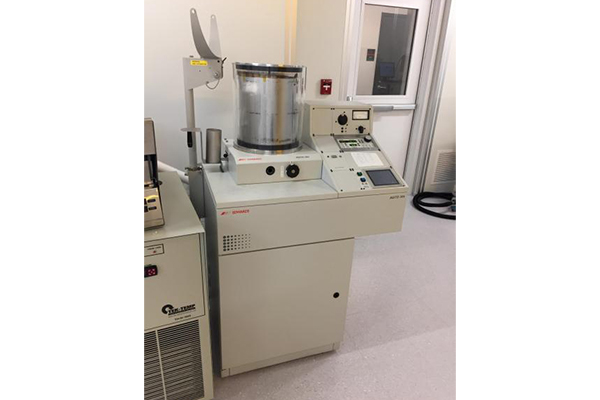
Atomic Layer Deposition | Savannah S100 Thermal ALD
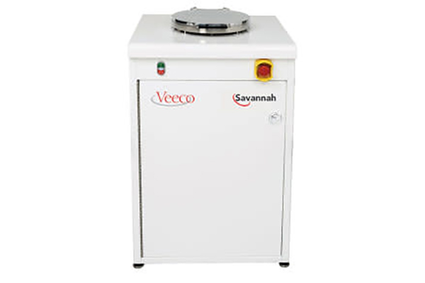
Veeco Savannah S100 Thermal Atomic Layer Deposition System
The Atomic Layer Deposition (ALD) system from Veeco (Model Savannah S100 Thermal ALD) can deposit several different kinds of materials with high conformality and at an atomic level (Angstrom) thickness control. Films can be deposited at up to 400 C. Currently, IMSE provides the capability of Al2O3 using Trimethyl Aluminum (TMA) precursor and water as co-reactants in the Al2O3 ALD process. Three additional precursors can be installed at same time on the instrument. Users are allowed to bring their own precursors. IMSE also provides the capability to measure thin film properties using ellipsometry, profilometry, SEM, TEM, XPS, resistivity, etc.
Book a Reservation/Equipment Availability - Request Training
IMSE Contact & Approved Trainer:
Recipe:
N/A
Technical Info:
Instrument Specifications
Potential Materials for growth
Asher | Asher

PE 50 Asher
PE 50 Asher, manufactured by Plasma Etch, uses Oxygen plasma to remove organic materials such as photoresist. It can be operated either in RIE mode or in soft Plasma Etching/Ashing mode. Other gases can be included to tweak etching/ashing performance. RF power of up to 100 W can be applied.
Book a Reservation/Equipment Availability - Request Training
IMSE Contact & Approved Trainer:
Training Documents:
NOTE: User must demonstrate skills to IMSE staff before independent use.
Operating instructions
Recipe:
N/A
Technical Info:
Instrument Specifications
Dicing Saw | Disco Model DAD 323
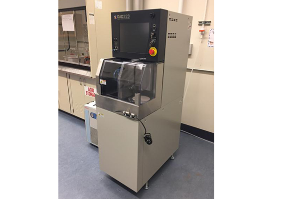
Disco Model DAD 323
The Disco DAD323 dicing saw can be used to cut a variety of materials such as silicon, glass, sapphire, etc. The substrate size is limited to 150 mm diameter and height to less than 5 mm. The rotating high speed blade makes a precise cut through the substrate which is mounted on adhesive tape. Samples should be able to withstand a high flow of water (water is used to keep the blade from getting hot). The instrument can run in manual mode or automatic mode to make repetitive cuts at precise spacing.
IMSE provides standard blades for cutting most types of materials and the cost is included in the instrument charges. Users are also allowed to bring their own. Currently, IMSE staff is responsible for changing the blades for all users.
Book a Reservation/Equipment Availability - Request Training
IMSE Contact & Approved Trainer:
Dr. Tyrone Daulton (tdaulton@wustl.edu)
Training Documents:
Operating Instructions NOTE: User must demonstrate skills to IMSE staff before independent use.
Recipe:
N/A
Technical Info:
Instrument Specifications
Disco Blade Z09 Specifications
Disco Blade R07 Specifications
E-beam Evaporator | AJA International
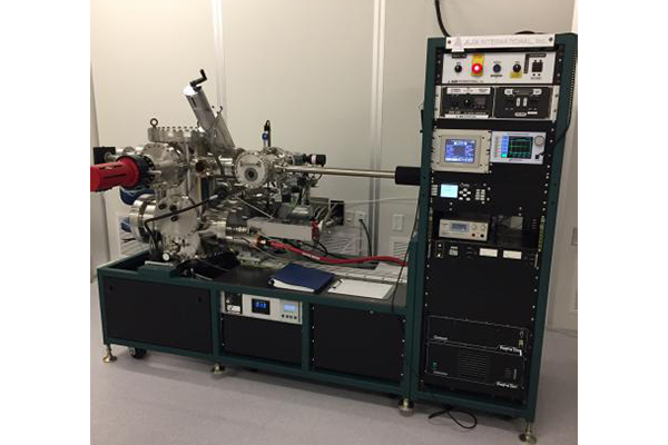
AJA International E-Beam Evaporator
The AJA International e-beam instrument can deposit materials for applications where high purity film and/or directionality of film growth is important. The deposition is done at very high vacuum ~1e-9 torr. Currently, the materials that can be deposited are: Al, AlO2, Nb, Ti. Oxygen gas is available to oxidize films in a controllable manner. Other materials are not possible due to conflicts with ongoing research and limitations in breaking the high vacuum condition. Deposition growth rate can range from 0.1 Angstrom/s to more than 4 Angstrom/s. If you need to deposit other materials, please contact IMSE staff.
Book a Reservation/Equipment Availability - Request Training
IMSE Contact:
Dr. Huafang Li (hli40@wustl.edu)
Approved Trainer:
Daria Kowsari (dariakowsari@wustl.edu)
Training Documents:
NOTE: User must demonstrate skills to IMSE staff before independent use.
Operating instructions
Recipe:
N/A
Technical Info:
N/A
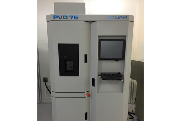
E-Beam Evaporator | Kurt J. Lesker PVD 75
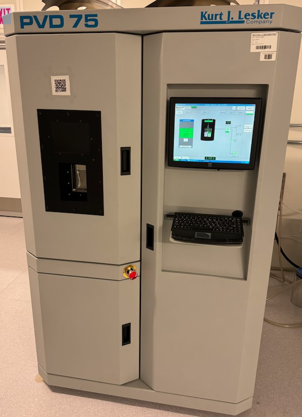
Kurt J. Lesker PVD 75 Electron Beam Evaporation
The Kurt J. Lesker PVD 75 thin film deposition system is a versatile platform equipped for electron-beam (4 pockets) evaporation. Electron beam evaporation stands out as the preferred method for high melting point materials, offering directional control advantageous for liftoff metallization. Meanwhile, the Lesker PVD 75 Electron Beam Evaporation apparatus employs this technique to deliver precise management of deposition rates, minimal contamination in films, and rapid deposition rates. It provides pellets for ebeam deposition including Al, Cr, Cu, Au, and Ti, with an upward evaporation orientation and four pockets for multilayer deposition. Monitoring film thickness is facilitated by a Quartz Crystal Microbalance (QCM), while accommodating substrates of up to 150 mm in size with rotation capabilities of up to 20 rpm.
Book a Reservation/Equipment Availability - Request Training
IMSE Contact & Approved Trainer:
Training Documents:
NOTE: User must demonstrate skills to IMSE staff before independent use.
Operating Instructions
Recipe:
Click here to see available recipes
Technical Info:
N/A
Ellipsometer | J.A. Woollam alpha-SE spectroscopic

J.A. Woollam alpha-SE spectroscopic
The J.A. Woollam alpha-SE ellipsometer can measure film properties non destructively. Some of the film properties include optical constants, film thickness and roughness. The change in polarized light properties during the measurement can measure film thickness from micrometer length scales down to angstrom length scales precisely. The instrument is typically used for dielectric, semiconductor and organic thin films.
The instrument has a wavelength range from 380 nm - 900 nm, and can operate at three angles (65, 70 and 75 degrees) in manual mode.
Book a Reservation/Equipment Availability - Request Training
IMSE Contact & Approved Trainer:
Recipe:
N/A
Technical Info:
Instrument Specifications
Heidelberg Laser Lithography System
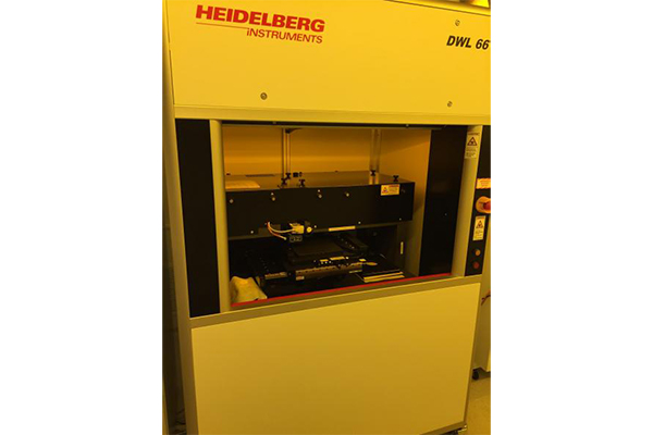
Heidelberg DWL66+ Laser Writer
The Heidelberg DWL66+ Laser writer provides advanced patterning applications using 375 nm UV laser to pattern a single resist layer by either simple exposure, front side aligned exposure, or back side aligned exposure. In addition, the writer can generate 3D patterns by using gray scale mode in which the intensity of the laser is varied while the laser is rastered. The smallest feature size that can be printed is better than 600 nm. The resist thickness can range from 100 nm to 100 micrometer. It can also be used to make photomasks for mask based lithography system.
Book a Reservation/Equipment Availability - Request Training
IMSE Contact & Approved Trainer:
Training Documents:
NOTE: User must demonstrate skills to IMSE staff before independent use.
AutoCAD guidelines
Operating instructions
Repeatability tests
Gray Scale (3D) patterning with Laser Lithography and RIE
Recipe optimization guidelines
Recipe:
Click here to see existing recipes
Technical Info:
Instrument Specifications
AZP4620 Resist datasheet
KL IR 15 Resist datasheet
S1805 Resist datasheet
SU8-2025 Resist datasheet
SU8-2050 Resist datasheet
Mask Aligner 3" | Karl Suss MJB3

Karl Suss MJB3
The Photolithography process transfers the patterned features from the mask on to the thin photoresist layer spin coated on silicon wafer. The Karl Suss MJB3 UV 400 mask aligner can provide a resolution down to 0.6 micrometer in optimal conditions. Considering the age of instrument, features size greater than 1 micrometer are reliably achievable. Photoresist layer thickness can be varied from sub micrometer to more than 200 micrometer depending on the photoresist material, spin coating speed and other process conditions. Selected photoresists (S1805 and SU-8 2050) are sold by IMSE in small quantities.
Book a Reservation/Equipment Availability - Request Training
IMSE Contact & Approved Trainer:
Training Documents:
NOTE: User must demonstrate skills to IMSE staff before independent use.
Operating instructions
Recipe:
Click here to see existing recipes
Technical Info:
AZP4620 Resist datasheet
KL IR 15 Resist datasheet
S1805 Resist datasheet
SU8-2025 Resist datasheet
SU8-2050 Resist datasheet
Mask Aligner 4" | Kloé SA
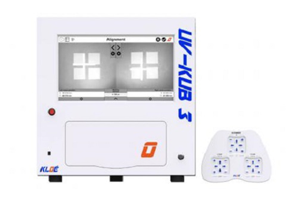
Kloé SA
An easy to use UV-LED mask aligner that can perform photolithography on substrates up to 4" diameter and with resolution as small as 2 microns. Front-side alignment can now be performed with joypad controls in a matter of minutes. It can be useful in many research applications not limiting it to microelectronics, microfluidics, optics & photonics.
Book a Reservation/Equipment Availability - Request Training
IMSE Contact & Approved Trainer:
Training Documents:
NOTE: User must demonstrate skills to IMSE staff before independent use.
Operating instructions
Recipe:
N/A
Technical Info:
Instrument Specifications
AZP4620 Resist datasheet
KL IR 15 Resist datasheet
S1805 Resist datasheet
SU8-2025 Resist datasheet
SU8-2050 Resist datasheet
Nanofab PECVD System | Oxford Instrument

Oxford Instrument
Oxford Instrument's Nanofab provides the capability to deposit thin films of SiO2, SiN, p-Si, a-Si, Graphene, Nanotubes, etc. The standard gasses connected to the instrument are Ar, N2O, N2, CH4, 2%SiH4 in Ar, NH3, and H2. For more process capability, please contact IMSE staff.
Book a Reservation/Equipment Availability - Request Training
IMSE Contact & Approved Trainer:
Training Documents:
NOTE: User must demonstrate skills to IMSE staff before independent use.
Operating instructions
Recipe:
Click here to see existing recipes
Technical Info:
Instrument Specifications
Optical Microscopes
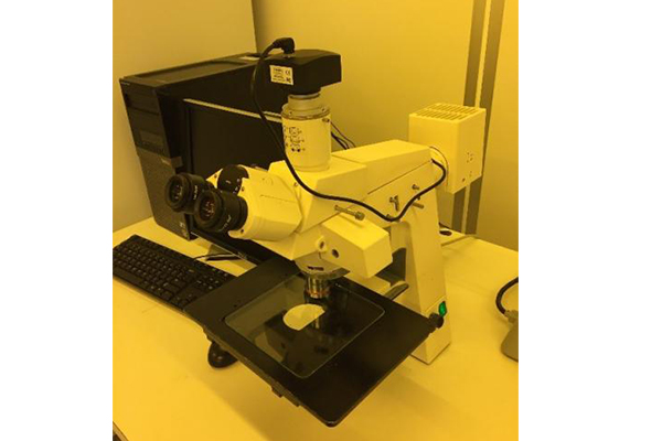
Zeiss AxioSkop Optical Microscope
The Optical microscope (Zeiss AxioSkop) in cleanroom (Class 100) can measure feature sizes below 1 micrometer. The following objective lenses are available: 5x, 10x, 20x, and 50x. Other applications include:
- Instrument is also useful in making a qualitative assessment on when the chemical development process during lithography has been successfully completed. Surface contrast and roughness helps in making the determination.
- Verifying undercut in a two-layer lithography process as part of metal layer patterning by a lift-off technique
Book a Reservation/Equipment Availability - Request Training
IMSE Contact & Approved Trainer:
Recipe:
N/A
Technical Info:
N/A
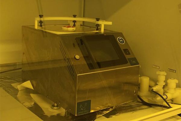
Parylene Deposition System | Specialty Coating Systems, PDS 2010 Labcoter
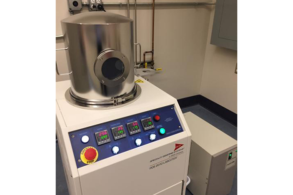
Specialty Coating Systems, PDS 2010 Labcoter
The SCS Parylene Deposition system (Model PDS 2010) can coat a very uniform coating of parylene film over a wide variety of substrates maintained at room temperature. The IMSE is currently providing Parylene-C dimer, however, other Parylene dimers can be explored in the system. It is used in a wide range of applications, including circuit boards, sensors, wafers, medical devices and elastomeric components for research, development and repair. This system is located in Rudolph Hall, L27, outside of the cleanroom.
Book a Reservation/Equipment Availability - Request Training
IMSE Contact & Approved Trainer:
Training Documents:
NOTE: User must demonstrate skills to IMSE staff before independent use.
Operating instructions
Recipe:
N/A
Technical Info:
Instrument Specifications
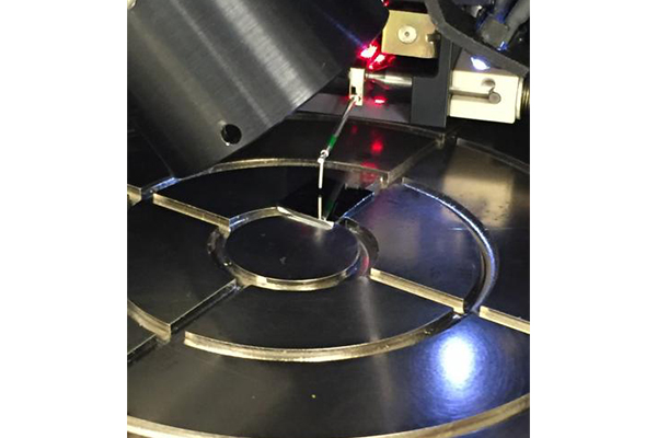
Probe Station | Signatone S-1008 and Keithley 238 high current source measurement unit
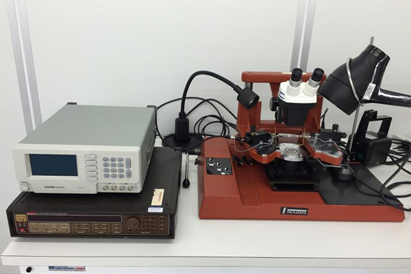
Signatone S-1008 and Keithley 238 high current source measurement unit
The Signatone S-1008 Probe station can be used to precisely measure substrate (or thin film on substrate) electrical properties using the Keithley 238 Source Measure Unit. Probes can be placed with sub-100 micron precision. 2-wire and 4-wire measurements are available. Probes are adjustable to meet different substrate size requirements. LCR 800 meter is also available for measuring additional electrical properties. Measurements can be taken in manual and automated manner.
Book a Reservation/Equipment Availability - Request Training
IMSE Contact & Approved Trainer:
Training Documents:
NOTE: User must demonstrate skills to IMSE staff before independent use.
Operating Instructions
Recipe:
N/A
Technical Info:
Keithley 238 Manual
LCR 800 manual
Profilometer | KLA-Tencor Alpha-Step D-100
KLA-Tencor Alpha-Step D-100
The KLA Tencor D-100 series profilometer measures the 2D surface topography, step height and thin film stress by using a stylus in close contact with the surface while maintaining the set force between the stylus and surface. 2D profiles can scan up to 30 mm in length. The technique is usually non-destructive except for very soft organic material based films.
Book a Reservation/Equipment Availability - Request Training
IMSE Contact & Approved Trainer:
Training Documents:
NOTE: User must demonstrate skills to IMSE staff before independent use.
Operating instructions
Recipe:
N/A
Technical Info:
Instrument Specifications
Reactive Ion Etch (RIE) | Oxford Plasma Lab 100 Inductively Coupled Plasma (ICP)
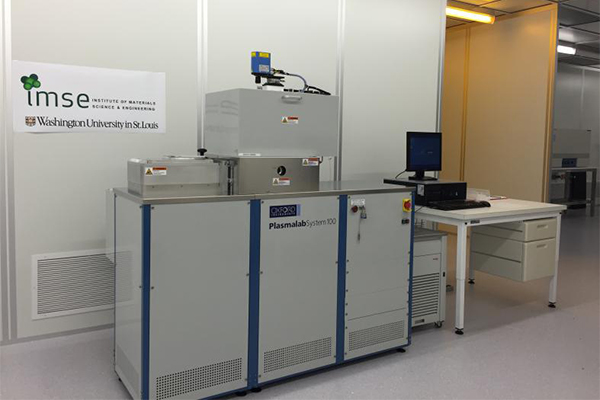
Oxford Plasma Lab 100 Inductively Coupled Plasma (ICP)
Oxford Instrument's Plasma Lab 100 System provides the capability to etch features on silicon wafers using plasma based gas chemistries. The instrument has dual source plasma: Inductive Couple Plasma (ICP) on top chamber and Reactive Ion Plasma source on Substrate. The tool has the ability to run ICP based deep Si etch processes. The standard gasses connected to the instrument are Ar, O2, He, CHF3, SF6, NF3, H2 and CH4.
Book a Reservation/Equipment Availability - Request Training
IMSE Contact & Approved Trainer:
Training Documents:
NOTE: User must demonstrate skills to IMSE staff before independent use.
Operating instructions
Recipe:
Click here to see the current recipes
Technical Info:
N/A
Solvent Fume Hoods

Solvent Fume Hood
The Solvent hood has the capability to handle any number of solvents and developers. This is one of two solvent hoods and is located in Cleanroom Class 100 room. Waste is handled in a controlled and safe manner. Additional DI water is available for high purity applications. Hot plates and ultrasonicator are included in the reservation. Typically, the area is used during the development process in Photolithography.
NOTE:
- If you perform overnight or long lift-off experiments (after approval from staff), please record actual usage time and mention lift-off in the comment. IMSE will only bill you for 30 min for lift-off experiments.
Book a Reservation/Equipment Availability - Request Training
IMSE Contact & Approved Trainer:
Training Documents:
NOTE: User must demonstrate skills to IMSE staff before independent use.
Personal Protective Equipment
Solvent Waste Handling
Recipe:
N/A
Technical Info:
Safety Data Sheets of chemicals
Following chemicals must use apron and face shield. Check SDS of each chemical to ensure PPE compliance and verify with staff.
2-butanone
Following chemicals can be heated during normal 8-5pm working hours. IMSE staff makes the determination of which chemical should be heated. Review SDS for each chemical.
Remover PG. Keep hot plate temperature < 60 CAZ400T - Photoresist stripper. Keep hot plate temperature < 80 C
Solvent Fume Hoods (outside of cleanroom)
Solvent Fume Hoods - located in Rudolph L27
The Solvent hood has the capability to handle any number of solvents and developers. There are two solvent hoods located in Lab L27 (outside cleanroom). Waste is handled in a controlled and safe manner. Additional DI water is available for high purity applications.
Book a Reservation/Equipment Availability - Request Training
IMSE Contact & Approved Trainer:
Training Documents:
NOTE: User must demonstrate skills to IMSE staff before independent use.
Operating instructions
Recipe:
N/A
Technical Info:
Safety Data Sheets of chemicals
Solvent Fume Hood - PDMS (outside of cleanroom)
Solvent Fume Hood - PDMS located in Rudolph L27
The PDMS Solvent hood has the capability to handle number of solvents and is dedicated for PDMS fabrication process. This is located in Lab L27 (outside cleanroom). Waste is handled in a controlled and safe manner. Additional DI water is available for high purity applications.
Weighing balance, oven and dessicator are provided to facilitate PDMS process.
Book a Reservation/Equipment Availability - Request Training
IMSE Contact & Approved Trainer:
Training Documents:
NOTE: User must demonstrate skills to IMSE staff before independent use.
Operating instructions
Recipe:
N/A
Technical Info:
Safety Data Sheets of chemicals
Spin Coater | Brewer Science CEE 200X
Brewer Science CEE 200X
The Brewer Science CEE 200X Spin Coater, located in Solvent Fume hood(1), can spin up to 6000 rpm with high accuracy and repeatability. The Windows based touch screen interface is highly user friendly to operate. Typically, it is used for Photolithography processes to deposit uniform film thickness on silicon substrate from few 10's of nanometer to 100's of micrometer depending on the selected resist material.
Book a Reservation/Equipment Availability - Request Training
IMSE Contact & Approved Trainer:
Training Documents:
NOTE: User must demonstrate skills to IMSE staff before independent use.
Operating instructions
Training Videos
Recipe:
Click here to see existing recipes
Technical Info:
Safety Data Sheets of chemicals
AZP4620 Resist datasheet
KL IR 15 Resist datasheet
S1805 Resist datasheet
SU8-2025 Resist datasheet
SU8-2050 Resist datasheet
MCC Primer 80/20
950 PMMA A8
Sputter Deposition Tool | Kurt J. Lesker PVD 75 RF and DC
Kurt J. Lesker PVD 75 RF and DC
The Kurt Lesker PVD 75 Physical Vapor Deposition system allows material deposition on substrates by sputtering material from a solid source (also called "target" material). A plasma based Ar sputtering process is used to deposit material of desired thickness at ~0.5 nm/s growth rates. In addition, reactive gases such as oxygen can be added to deposit oxides form of solid source material. Available target materials are: Al, SiO2, Niobium, SiN, ZnO, Cu, Zn, Ti. In addition, substrate can be heated to control deposited film properties.
Book a Reservation/Equipment Availability - Request Training
IMSE Contact & Approved Trainer:
Training Documents:
NOTE: User must demonstrate skills to IMSE staff before independent use.
Operating instructions
Training Videos
Recipe:
Click here to see existing recipes
Technical Info:
Quartz Crystal Microbalance (QCM) — Read Section 7.3 for calibration procedure and Appendix A for parameters for selected material.
Thermal Evaporator | Edwards 306 Vacuum Coater
Edwards 306 Vacuum Coater
The Edwards Auto 306 Vacuum coater deposits material in vacuum conditions by heating the source material. Films have low impurity due to high vacuum conditions. Growth rates are typically ~0.1 nm/s. Up to four materials can be deposited in-situ without breaking the vacuum. Users are expected to provide their own consumables, including boats and source materials.
Book a Reservation/Equipment Availability
IMSE Contact & Approved Trainer:
Training Documents:
NOTE: User must demonstrate skills to IMSE staff before independent use.
Operating instructions
Recipe:
Click here to see the current recipes
Technical Info:
Quartz Crystal Microbalance (QCM) — Read Section 7.3 for calibration procedure and Appendix A for parameters for selected material.
Tube Furnace | Lindberg/Blue M
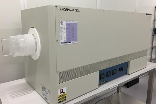
Lindberg/Blue M
Lindberg tube (glass)furnace can be heated up to 1100 C to grow oxide on silicon wafer under ambient conditions. Furnace is run in batch conditions. Typical SiO2 growth on Silicon substrate is ~430 nm for 15 hr run and ~820 nm for 80 hr run at 1100 C.
Book a Reservation/Equipment Availability - Request Training
IMSE Contact & Approved Trainer:
Training Documents:
NOTE: User must demonstrate skills to IMSE staff before independent use.
Operating Instructions
Training Videos
Recipe:
Click here to see available recipes
Technical Info:
N/A
UV Ozone Cleaner | UVOCS
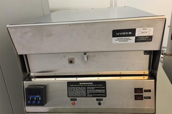
UVOCS
UVOCS UV based Ozone cleaner is used to clean remaining small residues on thin films surfaces such as silicon, gold and aluminum under ambient conditions. Cleaned surfaces can also be used to improve adhesion in certain processes. This is not meant to remove gross resist or organic surfaces with thickness greater than 100 nm. Gross material should be removed with wet chemistries. Certain halide residues are not allowed as they could corrode the interior parts.
Book a Reservation/Equipment Availability - Request Training
IMSE Contact & Approved Trainer:
Recipe:
N/A
Technical Info:
Instrument features