Facilities - equipment listing
Fabrication techniques
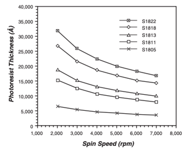
Spin coating
The process deposits thin film of organic material (typically photoresist) with desired film thickness on a Substrate. Substrate (or Silicon wafer) is spun at desired rotational speed (between 1000 rpm and 5000 rpm) for selected time (typically 45 sec). Spinning parameters are obtained from a data sheet supplied by manufacturer. An example Spin curve for S1805 Photoresist is shown below:
Step-by-Step illustration of Spin Coating Process:
|
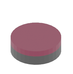
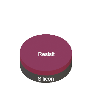
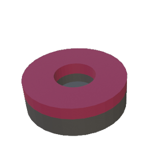
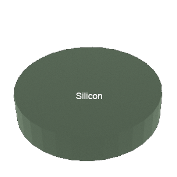
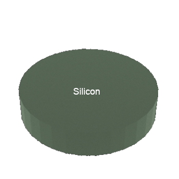
STEP 1: Start with Si wafer (substrate) |
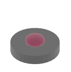
STEP 2: Drop few ml of resist on Si wafer |
|
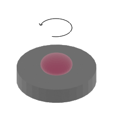
STEP 3: Rotate/Spin wafer at selected rpm |
STEP 4: Obtain desired film thickness of resist on Si wafer |
The above process can be carried out in IMSE Facility. Click here to learn more of our capability and start the training process.
Photo lithography
The process of photolithography uses photo light (UV light ~375nm wavelength) to pattern thin films of specialized organic materials (also known as photoresist or resist). Photoresist is a light sensitive material which changes in its chemical structure when exposed to UV light. Chemically modified photoresist is then removed in a chemical solution (also known as developer) to form a pattern of photoresist. Typically, a physical mask (also known as photomask) is used to control the exposed area of photoresist that sees a UV light.
Step-by-Step illustration of Photo Lithography Process:
|
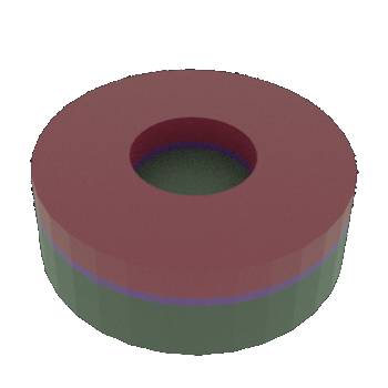
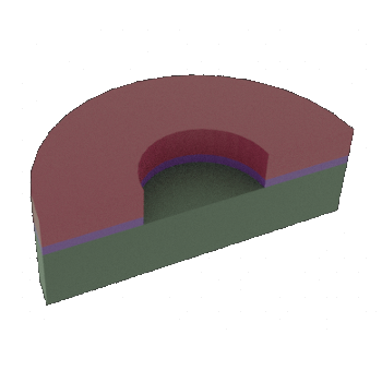
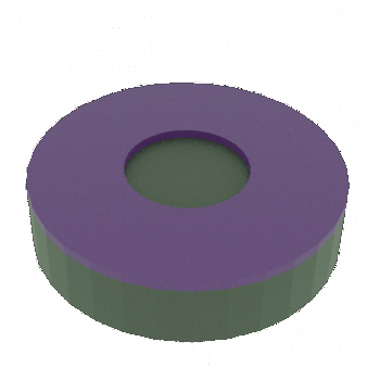
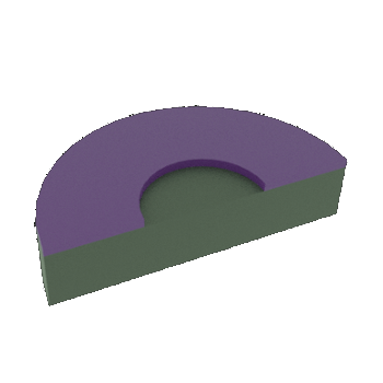
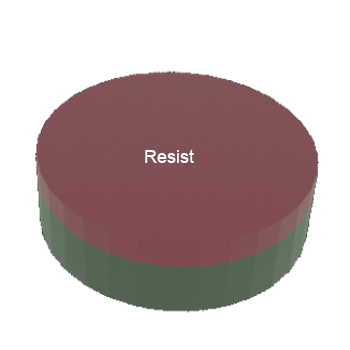
STEP 1: Start with Si wafer (substrate) with Resist on top |
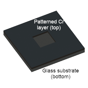
STEP 2: Purchase (or Fabricate) mask (Cr patterened on Glass) |
|
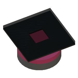
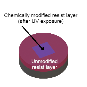
STEP 3: Flip mask and place on top of Resist coated Si. Typically, there is no separation between the two. Expose UV (~375nm) light above the glass mask (not shown in picture) |
STEP 4: Part of the resist exposed to UV light is chemically modified (shown in darker color) |
|
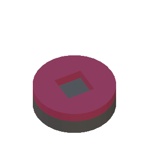
STEP 5(a): Substrate is kept in chemical solution (developer) (not shown). If chemically modified resist is removed after development, the process is called Positive lithography. |
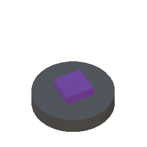
STEP 5(b): Substrate is kept in chemical solution (developer) (not shown). If chemically modified resist stays after development, the process is called Negative lithography. |
The above process can be carried out in IMSE Facility. IMSE offer two Mask aligners: MJB Mask Aligner and KLOE Mask Aligner. Click the links to start the training process.
Alternate to mask based Photo Lithography Process:
UV laser (375nm) is another alternative to mask based UV lithography. Here, the UV laser is rastered on the resist coated substrate. UV laser motion (or areas exposed) is controlled by a design drawn in AutoCAD. Laser based exposure is often a slower photolithography process ( ~ hours) in comparison to mask based exposure (~ min). However, the UV laser provides the repeatability and feature capability down to 0.6 micro. Most applications of UV laser lithography include designing a one time photomask (Resist/Cr/Glass) or writing features with size below 1 micro. IMSE offers the Heidelberg UV Laser Writerto accomplish this process. Click the link to learn more and start the training process.
Additional Links
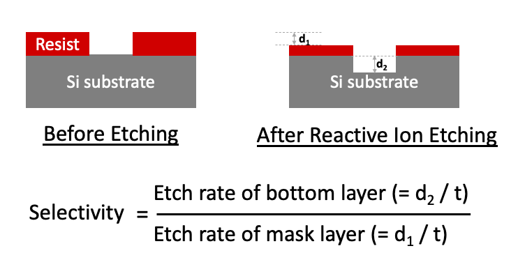
Reactive ion etching (dry etching) + wet etching
Reactive Ion etching (RIE) is the process of transferring pattering in a top mask layer (e.g. Resist) to a second bottom layer (e.g. Silicon) using a plasma of etching gases (e.g. CF4 gas). Plasma is formed when a high electric field breaks down the gas molecules to ions, neutral, and radicals. Typically, an electric field is directly applied to a substrate or wafer. These species are highly reactive and can etch thin film material in both chemical form or physical (sputtering) form. Chemical based etching occurs when reactant species (e.g. Fluorine radicals) react with material (e.g. Silicon) to form a byproduct (e.g. SiFx) which is volatile at room temperature and low pressure (~10 mtorr). Physical etching occurs when plasma ions are propelled under an electric field to strike thin film material at high velocity. In most cases, the combination of chemical and physical forms gives synergistics benefits in etch performance. For example, an etching profile can be anisotropic, or higher etch rates can be obtained for the same selectivity.
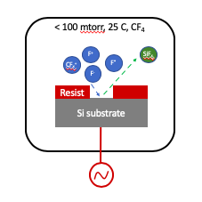
Since there is not a wet chemical in the RIE process, etching is sometimes referred to as Dry etching. Other synonyms of the process include - Plasma etching. Most advanced RIE systems come with dual plasma sources to achieve better control over the etch rate, selectivity and side wall angle. For example, IMSE RIE etching uses an Inductively Coupled Plasma (ICP) source on the top part of the chamber and a second Plasma source on the wafer. This configuration is often called ICP/RIE etching.
Ideally, a selected RIE etch process/chemistry will not damage (or erode) the top mask layer and will only remove the material in the second bottom layer. However, in the actual process the top mask layer is also etched. Plasma chemistry is selected to minimize the etch rate (i.e. film thickness etched per unit time) of the top mask layer and maximize the etch rate of the second bottom layer.
Selectivity is often used to define the ratio of etch rates of the two layers. Ideal Plasma etch conditions has a selectivity >> 1.
 Step-by-Step illustration of Wet Etching Process:
|
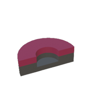
STEP 1a: Start with Si wafer (substrate) with Resist on top |
STEP 1b: Cross-sectional view of Step 1a |
|
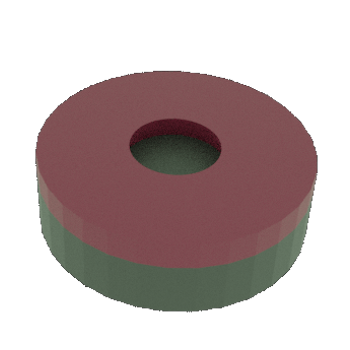
STEP 2a: Pattern photoresist using photolithography process (steps not shown) |
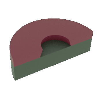
STEP 2b: Cross-sectional view of Step 2a |
|
STEP 3a: After substrate is etched in RIE etcher (not shown). |
STEP 3b: Cross-sectional view of Step 3a |

The above process can be carried out in the IMSE Facility. IMSE offers the Oxford RIE etcher to accomplish the task safely. Click the link to start the training process.
Thin film metrology
Estimating etch performance (etch rate, planar roughness, side wall roughness, etc.) is critical to fabricating devices at the micron scale in a repeated manner. IMSE offers a number of instruments ( Profilometer, Optical Microscope, Ellipsometer, SEM) to help in the quantitative measurements.
- Optical microscopes can measure the critical dimension width. Qualitative images can help in determining whether the film is completely removed.
- Profilometers can measure the height of thin film as long as a step edge is available in a patterned region. The instrument may also be used to estimate the roughness of etched films.
- Ellipsometer can measure the film thickness of selected materials when deposited on Silicon substrate. Unlike a profilometer, no patterned region should exist in the area of measurement.
Alternate to wet-etching Process:
The major disadvantage with wet-etching is the loss of critical dimensions due to isotropic nature of wet etching process. For example, 5 micron wide trench in resist may turn out to be 10 micron wide in etched layer underneath. As an alternate, Plasma based dry etching process is useful in preventing this loss of critical dimensions by keeping etching process anisotropic.
Limitations of RIE Process:
Certain materials (such as Gold) do not form etch byproducts with sufficient vapor pressure, and hence do not etch easily. Metal etch processes can also leave residue in parts of the etching chamber. These residues can cause yield issues when etching other materials (such as SiO2). For these reasons, the IMSE limits metals that can be etched or used as a mask in the Oxford RIE instrument.
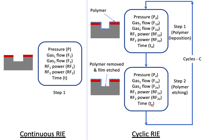
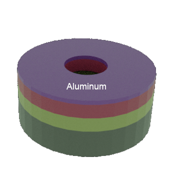
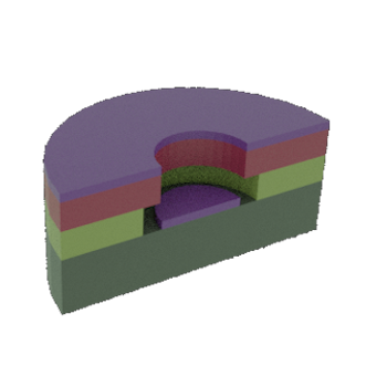
Deep Si RIE etch (cyclic) process
Continuous RIE process as explained above are typically used to etch thin films with thickness less than 50 microns. As films are etched deeper, it becomes difficult to maintain high selectivity and vertical sidewalls in patterned structures. The Deep RIE process overcomes this limitation by using a two-step cyclic process where one step is used to deposit thin polymer film (using C4F8 gas) and a second step is used to remove the polymer (using SF6 gas) at bottom of etched structure. A pair of two steps constitutes 1 cycle and is repeated (or number of cycles) to get the desired etch depth. Repeated processes leads to additional roughness on the sidewalls. These are also called as scallops.
Typically, this process is used to partially etch Si substrate with thickness > 100 um, and sometimes to completely etch a hole (or feature) in Si substrate. Other synonymous names of Deep Si etch include Bosch etch, Deep etch, Bosch RIE.
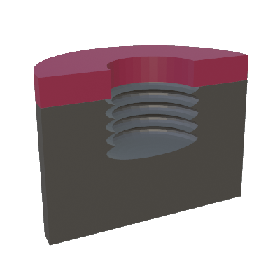 Formation of scallops during Deep Si RIE process
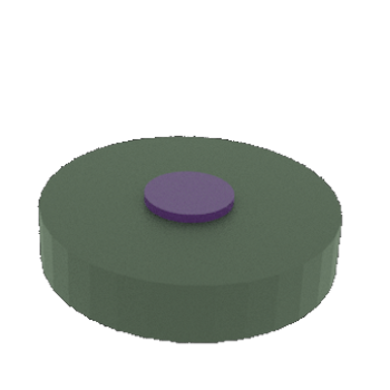
Metal deposition (sputtering)
Metal Deposition by Sputtering starts with creating high electrical field around source material (or target) of interest. Electrical field creates Plasma and removes material atoms from the source material. These removed material is then deposited on substrate of interested. High mean free path in vacuum ensures that most sputtered (or removed material) is deposited on the substrate of interest.
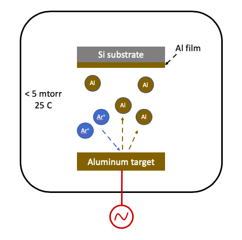
Plasma source can be either RF or DC. Typically, DC source is used for metal (or electrically conducting) source (or target) material, and RF source is used for insulator source (or target) materials. Ar is primarily the source gas as it is easy to ionize and create plasma. For certain use cases, oxygen can be mixed with Ar to deposit oxide forms on metal source.
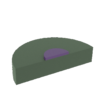
Step-by-Step illustration of Metal Deposition Process:
|
STEP 1: Start with Si wafer (substrate) |
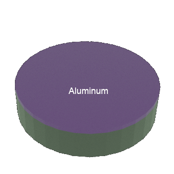
STEP 2: Si wafer (substrate) with Aluminum thin film on top |
The above process can be carried out in IMSE Facility. IMSE offers Sputter Deposition Tool to accomplish the task safely. Click the link to start the training process.
Thin film metrology
Estimating film deposition performance (deposition rate, planar roughness, side wall roughness, etc.) is critical to fabricate device at micron scale in repeated manner. IMSE offers number of instruments ( Profilometer, Optical Microscope, In-situ Quartz Crystal Microbalance (QCM) Sensor, SEM) to help in the quantitative measurements.
- Optical microscope can measure the critical dimension width (for patterned thin films)
- Profilometer can measure the thin film height as long as step edge is available. The simplest solution may be to cover part of planar surface with kapton tape during metal deposition. Instrument may also be used to estimate roughness of deposited films.
- In-situ QCM sensor can measure the thickness deposited on substrate in real-time. However, the sensor must be calibrated against another metrology (for example, Profilometer) before using for measurement.
Metal deposition (E-beam)
Metal Deposition by E-beam uses an electron beam to heat the material of interest and creates sufficient vapor pressure of the material in vacuum. E-beam is generated by thermionic emission (heating filament at high enough temperature to extract electrons) or field emission (using high electric field to extract electrons). E-beam is accelerated using controlled electric and magnetic field, and made to strike at the material of interest. Typically, the material is used in small pellet form (e.g. 1mm size) and kept inside/top of crucible (e.g. Boron Nitride ceramic). The crucible is kept at room temperature with water cooling underneath to prevent it from getting hot. The crucible material is selected such that it has a higher melting point and that does not form an alloy with material of interest. The evaporated material is then deposited on substrate of intereste. High mean free path in vacuum ensures that most evaporated material is deposited on the substrate of interest.
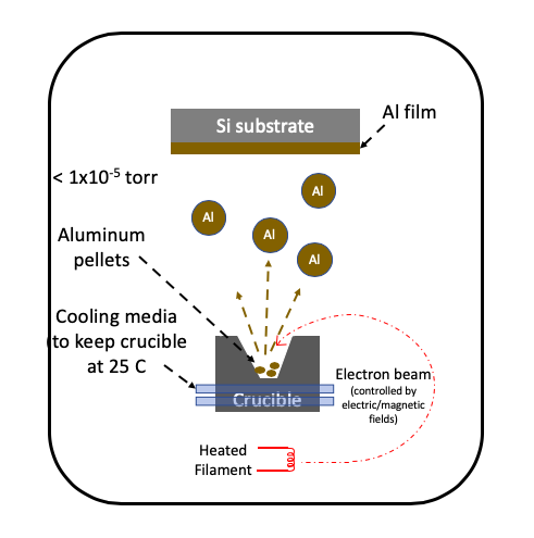
Comparison with Thermal Evaporation:
Thermal evaporation process heats the boat to a very high temperature, and hence the boat material can potentially contaminate the deposited film. However, in the E-beam deposition process, only the material of interest is heated. The boat is kept at room temperature at all times, and which gives a very high purity thin film. The E-beam technique can also deposit metals which may form alloys at high temperature with boat. For example, Platinum can be deposited by E-beam technique but not by Thermal evaporation.
Step-by-Step illustration of Metal Deposition Process:
|
STEP 1: Start with Si wafer (substrate) |
STEP 2: Si wafer (substrate) with Aluminum thin film on top |
The above process can be carried out in the IMSE Facility. IMSE offers AJA E-beam Evaporator to accomplish the task safely. Click the link to start the training process.
Thin film metrology
Estimating film deposition performance (deposition rate, planar roughness, side wall roughness, etc.) is critical to fabricate a device at micron scale in repeated manner. IMSE offers a number of instruments ( Profilometer, Optical Microscope, In-situ Quartz Crystal Microbalance (QCM) Sensor, SEM) to help in the quantitative measurements.
- Optical microscope can measure the critical dimension width (for patterned thin films)
- Profilometer can measure the thin film height as long as a step edge is available. The simplest solution may be to cover part of planar surface with kapton tape during metal deposition. Instrument may also be used to estimate roughness of deposited films.
- In-situ QCM sensor can measure the thickness deposited on substrate in real-time. However, the sensor must be calibrated against another metrology (for example, Profilometer) before using it for measurement.
Metal patterning
Metal Patterning is a process of patterning thin metal films using a combination of metal deposition, metal removal, and photolithography. The two widely used methods are:
- Subtractive Transfer - Resist layer is patterned on top of metal thin film. Exposed metal film is then etched with wet etchant, and followed by removal of resist to give a patterned metal layer.
- Additive Transfer (lift-off method) - Metal is deposited over patterned resist layer. Resist layer is then removed (or lifted off) to give patterned metal layer. Single layer of resist may be replaced with two layers of resist for better repeatability of lift-off process.
The above process can be carried out in IMSE Facility. IMSE offers Fume hoods, Lithography and Metal deposition instruments to accomplish the task safely. Click the link to start the training process.
Step-by-Step illustration of Metal Deposition using Subtractive Transfer Process:
|
STEP 1: Start with Si wafer (substrate) |
STEP 2: Si wafer (substrate) with Aluminum thin film on top |
|
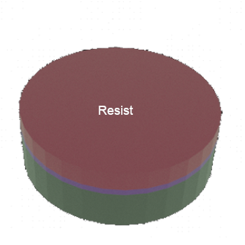
STEP 3: Al/Si wafer (substrate) with Resist thin film on top |
|
|
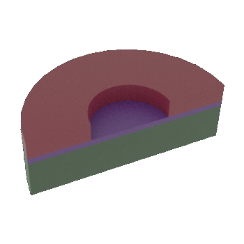
STEP 4a: Al/Si wafer (substrate) with patterned Resist thin film on top (lithography steps not shown) |
STEP 4b: Cross-sectional view of 4a |
|
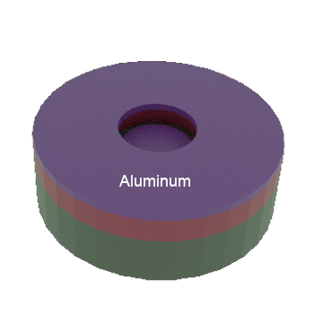
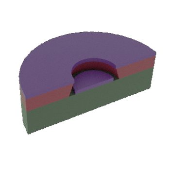
STEP 5a: Exposed Al removed by Wet etching |
STEP 5b: Cross-sectional view of 5a (Undercut in Al layer not shown) |
|
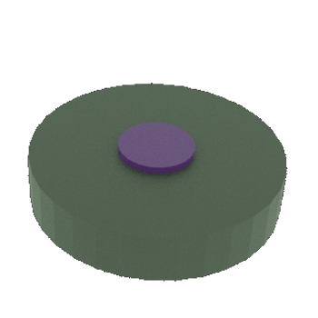
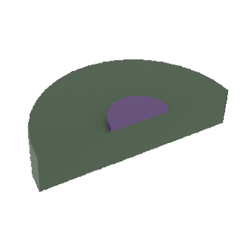
STEP 6a: Patterned metal layer after Resist layer is removed |
STEP 6b: Cross-sectional view of 6a |

Step-by-Step illustration of Metal Deposition using Additive Transfer Process with Single layer resist:
Typically, the resist selected is negative resist to give a negative profile which helps in lift-off process.
|
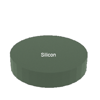
STEP 1: Start with Si wafer (substrate) |
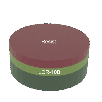
STEP 2: Si wafer (substrate) with two layers of resist on top |
|
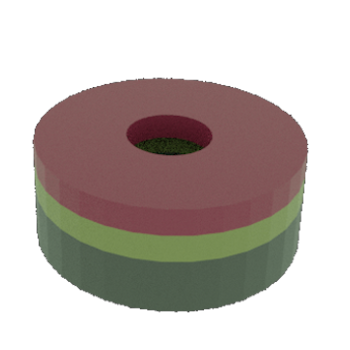
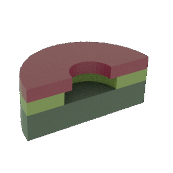
STEP 3a: Patterned (both) Resist layer on top (lithography steps not shown) |
STEP 3b: Cross-sectional view of 3a (NOTE: Undercut in LOR-10B layer depends on development time) |
|
STEP 4a: After aluminum metal deposition (equipment steps not shown) |
STEP 4b: Cross-sectional view of 4a |
|
STEP 5a: Patterned metal layer after Resist layer is lift-off in wet solution |
STEP 5b: Cross-sectional view of 5a |
Step-by-Step illustration of Metal Deposition using Additive Transfer Process with two layer resist:
In two layer process, first resist layer is LOR-10B and second layer is positive (or negative) resist. Developer solution used for second layer resist also removes exposed LOR-10B layer.
|
STEP 1: Start with Si wafer (substrate) |
STEP 2: Si wafer (substrate) with single layer of resist on top |
|
STEP 3a: Patterned Resist layer on top (lithography steps not shown) |
STEP 3b: Cross-sectional view of 3a |
|
STEP 4a: After aluminum metal deposition (equipment steps not shown) |
STEP 4b: Cross-sectional view of 4a (NOTE: Negative profile in resist layer) |
|
STEP 5a: Patterned metal layer after Resist layer is lift-off in wet solution |
STEP 5b: Cross-sectional view of 5a |
Thin film metrology
Estimating metal pattern performance (critical dimensions change, feature widths, planar roughness, side wall roughness, etc.) is critical to fabricate device at micron scale in repeated manner. IMSE offers number of instruments (Profilometer, Optical Microscope, SEM) to help in the quantitative measurements.
- Optical microscope can measure the critical dimension width (for patterned thin films)
- Profilometer can measure the thin film height as long as step edge is available. Instrument may also be used to estimate roughness of etched films.
Thermal oxidation
Thermal oxidation is typically done to oxidize Silicon in air at high temperature (~1100 C). At such high temperature, oxygen reacts with Silicon to form Silicon Dioxide. As Silicon is oxidizing, Oxygen reaching the unoxidized Silicon layer is reducing and controlled by process of Diffusion. Hence, the rate of oxidation decreases with time.
Air may be replaced with other gases such as pure oxygen, mixture of oxygen with inert gases, or water vapor. Air flow can be controlled or the process can even run in stagnant mode (i.e. no air flow). Typically, the process is carried out at ambient pressure.
The above process can be carried out in IMSE Facility. IMSE offers Tube Furnace to accomplish the task safely. Click the link to start the training process.
Thin film metrology
Estimating oxidation performance (oxidation rate, planar roughness, etc.) is critical to fabricate device at micron scale in repeated manner. IMSE offers number of instruments ( Ellipsometer, Profilometer, Optical Microscope, SEM) to help in the quantitative measurements.
- Optical microscope can measure the critical dimension width (for patterned thin films)
- Profilometer can measure the thin film height as long as step edge is available. The simplest solution may be to cover part of planar surface with kapton tape during metal deposition. Instrument may also be used to estimate roughness of etched films.
- Ellipsometry can measure the film thickness of selected materials when deposited on Silicon substrate. Unlike profilometer, no patterned region should exist in the area of measurement.
Chemical vapor deposition
Chemical Vapor Deposition (CVD) uses one or more volatile precursors to deposit high quality thin films on desired substrates. Substrate is heated to desired temperature (650 C) to create chemical reaction from substrates. For example, Tetraethylorthosilicate precursor in vapor form will decompose at a high temperature on substrate to deposit Silicon Dioxide thin film. CVD process is carried out in vacuum to obtain uniform deposition and high purity films.
Many standard precursors are available today that can deposit metals, silicon oxide, silicon, silicon nitride, etc by CVD process. The precursor must be volatile, leave no impurity in deposited films, and give desired film properties (such as uniformity, electrical resistance, roughness, etc.). All byproducts from CVD surface reaction should be volatile and easily removable in vacuum. Precursors should not react among each other in vapor form, and only react at high temperature maintained at substrate.
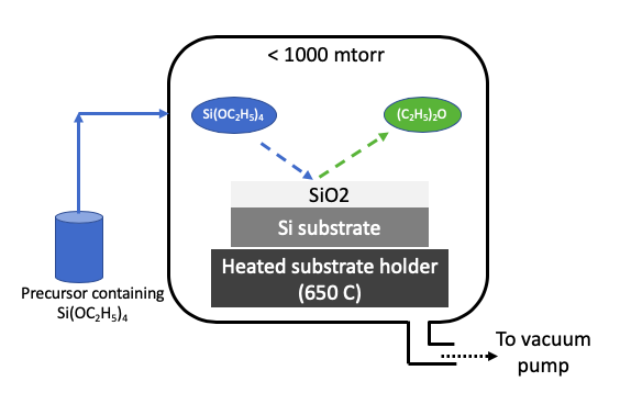
The above process can be carried out in IMSE Facility. IMSE offers Nanofab PECVD system to accomplish the task safely. Click the link to start the training process.
Thin film metrology
Estimating film growth performance (deposition rate, planar roughness, etc.) is critical to fabricate the device at micron scale in a repeated manner. IMSE offers a number of instruments ( Ellipsometer, Profilometer, Optical Microscope, SEM) to help in the quantitative measurements.
- Optical microscope can measure the critical dimension width (for patterned thin films)
- Profilometer can measure the thin film height as long as a step edge is available. The simplest solution may be to cover part of planar surface with kapton tape during metal deposition. Instrument may also be used to estimate roughness of etched films.
- Ellipsometry can measure the film thickness of selected materials when deposited on Silicon substrate. Unlike profilometer, no patterned region should exist in the area of measurement.
Graphene deposition
Graphene can de deposited on Cu thin substrate by flowing Methane and Hydrogen at high temperature (1200 C). Cu surface cleanliness is equally critical for deposition. Nanofab PECVD system at IMSE has established recipes to perform this sensitive process.
Plasma enhanced chemical vapor deposition (PECVD)
Plasma Enhanced Chemical Vapor Deposition (CVD) uses plasma of ionized species to break one or more stable volatile precursors to deposit high quality thin films on desired substrates. Plasma is created by applying high RF electric field around the area near the substrate. Plasma is widely known to break stable molecules that would have otherwise taken much higher thermal energy (or temperature) to break. These reactive plasma species deposit on heated substrate to deposit thin film of interest. Unlike CVD which uses only thermal energy on substrate, PECVD process uses both energy from plasma and thermal energy on substrate to achieve desired chemical reaction for thin film growth. For example, Silane and Nitrous Oxide can deposit SiO2 films at 280 C using PECVD process. The same chemistry using a CVD process would have taken more than 800 C to grow SiO2 film. Lower temperature also permits deposition on substrates that may not withstand higher temperatures. Plasma can also help controlling stress in the thin films.
Many standard precursors are available today that can deposit metals, silicon oxide, silicon, silicon nitride, etc by PECVD process. Precusor must be volatile, leaves no impurity in deposited films, and give desired film properties (such as uniformity, electrical resistance, roughness, etc.). All byproducts from PECVD surface reaction should be volatile and easily removable in vacuum.
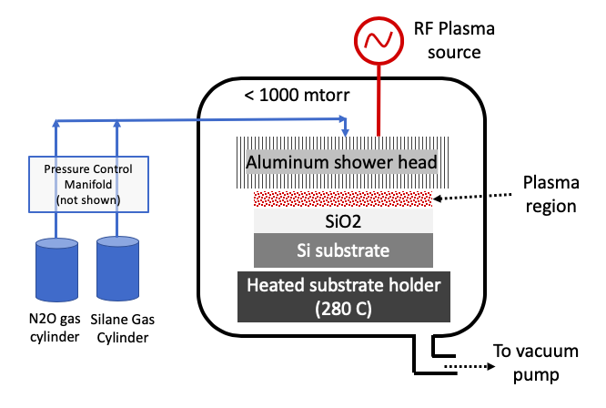
The above process can be carried out in IMSE Facility. IMSE offers (Nanofab PECVD system) to accomplish the task safely. Click the link to start the training process.
Thin film metrology
Estimating film growth performance (deposition rate, planar roughness, etc.) is critical to fabricate device at micron scale in repeated manner. IMSE offers number of instruments ( Ellipsometer, Profilometer, Optical Microscope, SEM) to help in the quantitative measurements.
- Optical microscope can measure the critical dimension width (for patterned thin films)
- Profilometer can measure the thin film height as long as step edge is available. The simplest solution may be to cover part of planar surface with kapton tape during metal deposition. Instrument may also be used to estimate roughness of etched films.
- Ellipsometry can measure the film thickness of selected materials when deposited on Silicon substrate. Unlike profilometer, no patterned region should exist in the area of measurement.
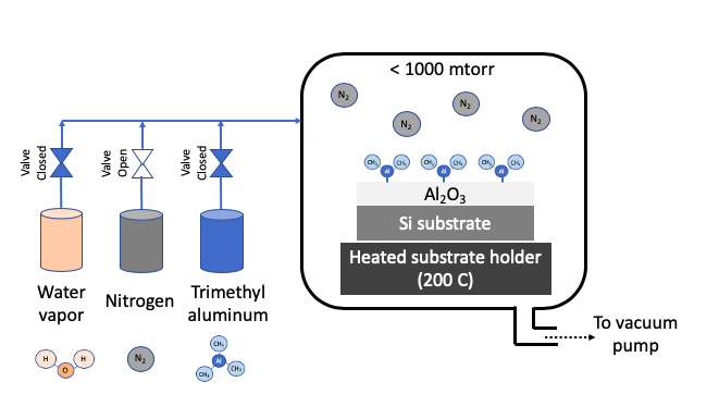
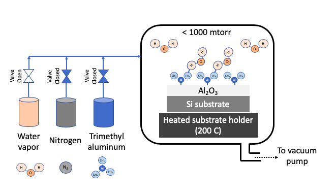
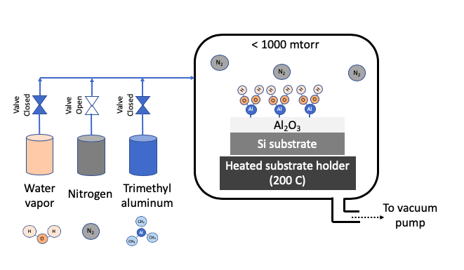
Atomic layer deposition (ALD)
Atomic Layer Deposition (ALD) uses one or more volatile precursors or gases to deposit high quality thin films on desired substrates with precision controlled at angstrom length scale. Unlike a CVD process which uses continuous flow of gases, the ALD process introduces precursors in the chamber in a sequential manner. Sequential approach and chemistry selection ensures that each precursor only forms a single monolayer at a time. For example, Al2O3 is deposition by first flowing Trimethyl aluminum precursor, then purging chamber with nitrogen, then flowing water vapor as second precursor, and then purging with nitrogen again. These four steps constitute 1 ALD cycles, and gives a growth rate of ~1 Angstron per cycle. A cycle is repeated to get the desired film thickness. Nitrogen purge between the steps of ALD cycle prevents an undesired reaction in vapor phase. The ALD process can deposit films in a highly uniform manner in any size or shape especially when repeatability is critical at angstrom length scale. ALD precursors are carefully selected to foster desired ALD chemistry on heated substrate. Substrate is typically heated to a desired temperature (100 - 350 C) to create chemical reaction on substrates. ALD process is carried out in vacuum to obtain uniform deposition and high purity films.
Many standard precursors are available today that can deposit metals, metal oxides, silicon oxide, etc by ALD process. The precusor must be volatile, leave no impurity in deposited films, and give desired film properties (such as uniformity, electrical resistance, roughness, etc.). All byproducts from ALD surface reaction should be volatile and easily removable in vacuum. Precursors should not react among each other in vapor form, and only react at high temperature maintained at substrate.
The above process can be carried out in IMSE Facility. IMSE offers ALD Instrument to accomplish the task safely. Click the link to start the training process.
Step-by-Step illustration of steps in 1 ALD Cycle:
|
STEP 1: Passivate surface with Precursor 1 (Trimethyl aluminum) |
STEP 2: Remove excess Precursor 1 with Nitrogen purge |
|
STEP 3: Introduce Precursor 2 (water vapor) to complete surface reaction |
STEP 4: Remove excess Precursor 2 with Nitrogen purge |

Thin film metrology
Estimating film growth performance (deposition rate, planar roughness, etc.) is critical to fabricate the device at micron scale in a repeated manner. IMSE offers a number of instruments ( Ellipsometer, Profilometer, Optical Microscope, SEM) to help in the quantitative measurements.
- Optical microscope can measure the critical dimension width (for patterned thin films)
- Profilometer can measure the thin film height as long as step edge is available. The simplest solution may be to cover part of planar surface with kapton tape during metal deposition. Instrument may also be used to estimate roughness of etched films.
- Ellipsometry can measure the film thickness of selected materials when deposited on Silicon substrate. Unlike a profilometer, no patterned region should exist in the area of measurement.